
Samsung Electronics recently announced a major technological breakthrough and future vision, which is its plan to apply FinFET process technology to NAND Flash memory production. This action is interpreted as Samsung's preparation to respond to...
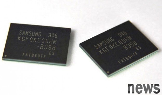
Samsung Electronics recently announced a major technological breakthrough and future vision, which is its plan to apply FinFET process technology to NAND Flash memory production. This action is interpreted as Samsung's preparation to respond to the demand for larger-capacity NAND Flash memory in artificial intelligence (AI) chipsets. However, this technology belongs to the future and practical application will still take some time.
SEDEX 2025, Song Jae-hyuk, chief technology officer of Samsung's DS department, gave a keynote speech and said that he is committed to technological innovation and the goal is to achieve the performance and power expected by customers within the unit area where transistors must be stacked. Among them, FinFET technology is one of the cores of this innovation strategy. FinFET is a 3D structure process technology. Because its structure is similar to a fish fin (Fin), it is named FinFET. The main purpose of Samsung's introduction of this technology is to overcome the limitations of traditional planar (2D) structures.
FinFET is mainly used in wafer foundry (Foundry) and is expected to be equipped with 3D DRAM. This time Samsung announced its plan to apply FinFET to NAND Flash memory, which is the first time in the industry. The semiconductor industry generally believes that once FinFET is applied to NAND Flash memory, the integration density will be significantly increased compared with existing memories. Moreover, the higher the density, the more components can be accommodated in a smaller space, further significantly improving performance.
Samsung Electronics confirms for the first time that it plans to apply 3D “FinFET” process technology to NAND flash.
Samsung Electronics is set to apply FinFET (Fin Field-Effect Transistor) technology to NAND flash memory. This move is interpreted as part of an effort to produce… pic.twitter.com/UA6tKoodkO
— Jukan (@Jukanlosreve) October 22, 2025
Samsung pointed out that the advantages brought by high density also cover many aspects. Including faster signal transmission, lower power consumption, and smaller chip size, helping to use space more efficiently. In other words, compared with the existing planar process, NAND Flash memory using the FinFET process not only has a larger capacity, but will also be faster.