The Russian Academy of Sciences recently released the blue map of the development of extreme ultraviolet (EUV) lithography tools from 2026 to 2037, planning to replace traditional deep ultraviolet (DUV) lithography technology. The core of the projec...
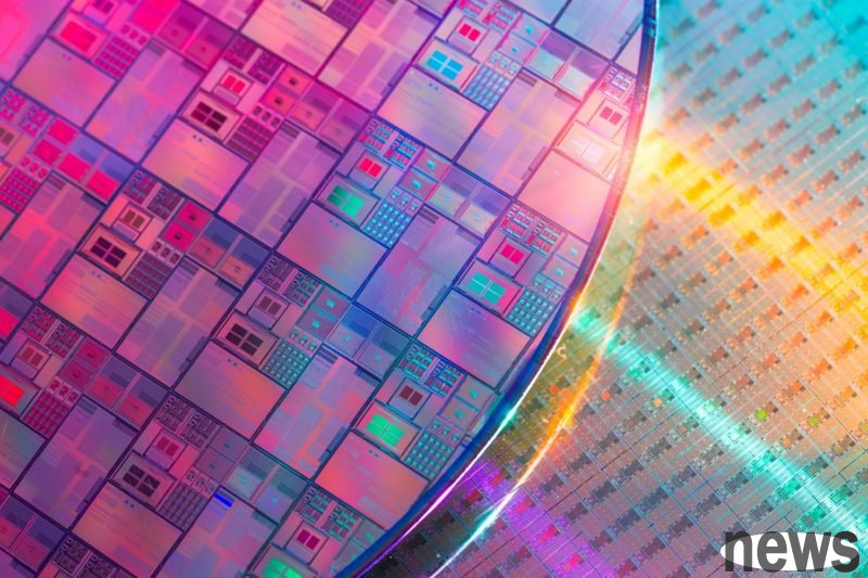
The Russian Academy of Sciences recently released the blue map of the development of extreme ultraviolet (EUV) lithography tools from 2026 to 2037, planning to replace traditional deep ultraviolet (DUV) lithography technology.
The core of the project is to develop an EUV direct-printed coverless film lithography system with a wavelength of 11.2 nanometers, using ionic light sources such as xenon gas and lamellae surfaces. Compared with the current ASML 13.5 nanometer wavelength equipment, Russia aims to provide a simpler and more cost-effective solution.
The plan is implemented in three stages: basic components development, and the launch of prototypes that support 200 mm crystal circles, and finally a mass production machine with 300 mm crystal circles. In May 2024, the first lithography machine capable of manufacturing chips with a maximum of 350 nanometers has been successfully installed and entered the test stage, and has set a stage goal of further supporting the 130 nanometers process in 2026. Technically, the Russian R&D team conducted simultaneously in the design of photoresist (especially organic silicon-based photoresist) and the customization of optical components, aiming to build a complete EUV lithography ecosystem.
However, experts are cautious about the feasibility of this plan. EUV lithography technology requires large funds and deep technical expenditure. Even if the technology is strong, the United States and Japan will be difficult to challenge the global failure of ASML. Whether Russia can cross technical and industrial capacity within ten years remains to be seen.
This breakthrough demonstrates Russia's determination in semiconductor autonomy and is expected to impact the global lithography technology landscape. If successful, it will promote the diversification of lithography technology routes in many countries, including electron beam micrograph, X-ray lithography, etc., and global industries may welcome more competition and innovation.
Russia outlines EUV litho chipmaking tool roadmap through 2037 — country eyes replacing DUV with EUV, but plans appear unrealistic